A Step Recovery Diode (SRD) is a special type of semiconductor diode also called as snap-off diode, charge storage diode and memory varactor diode. Step recovery diodes are having a different style of doping. It is not like a normal PN junction diode, it is a voltage dependent variable capacitor.

The density of charge carrier holes and electrons is very negligible near the junction. The density of charge carriers gradually increases as we move away from the junction. Since there are very small number of charges near the junction the switching speed of SRD is very fast.
known for its ability to generate extremely fast pulses. These diodes are utilized in high-frequency applications, such as pulse shaping, frequency multiplication, and harmonic generation, due to their unique charge storage and rapid charge recovery characteristics.

Working Principle of SRD:
The primary function of an SRD is based on its ability to store and release charge. During the forward bias, charge carriers (electrons and holes) are injected into the diode’s junction region. When the bias is reversed, these carriers are rapidly swept out, leading to a swift transition from a conductive to a non-conductive state. This transition is what gives the SRD its name and is key to its performance in high-speed applications.
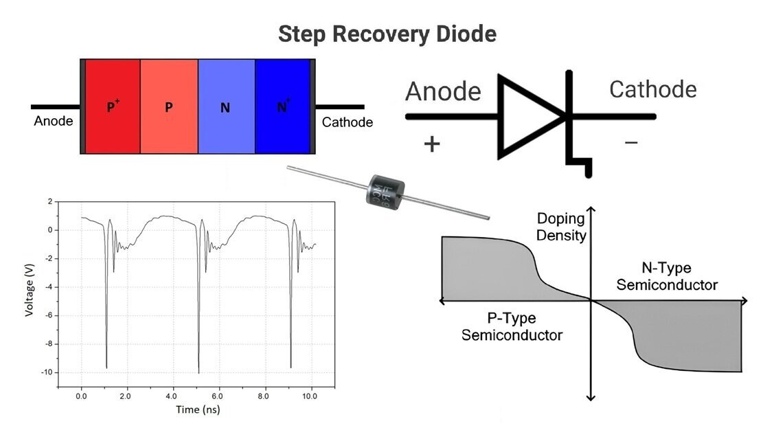
Construction of Step Recovery Diode:
The construction of a Step Recovery Diode (SRD) is meticulously designed to optimize its ability to store and rapidly release charge carriers, which is crucial for its high-speed switching capabilities. Below is a detailed overview of its construction:
Materials and Doping:
Semiconductor Material:
The SRD is typically made from silicon due to its favorable semiconductor properties. In some high-frequency applications, materials like gallium arsenide (GaAs) may be used due to their higher electron mobility.
Doping Profile:
N-Type Region: This region is lightly doped with donor impurities to create a high-resistance material.
P-Type Region: This region is lightly doped with acceptor impurities.
Abrupt Junction: The key feature of the SRD is the abrupt P-N junction created by the sharp change in doping concentrations between the P-type and N-type regions. This abrupt junction is critical for the diode’s fast charge recovery characteristics.
Layer Structure:
N+ Region (Heavily Doped N-Type):
Located at the anode end, this region is heavily doped to provide a low-resistance contact. It facilitates efficient injection of electrons into the diode during forward bias.
Intrinsic Region (Lightly Doped N-Type):
Adjacent to the N+ region, this intrinsic (or lightly doped) region forms the bulk of the diode. It plays a significant role in charge storage during forward bias operation.
P+ Region (Heavily Doped P-Type):
This region is heavily doped and located at the cathode end, providing a low-resistance contact for holes.
Depletion Region:
At the P-N junction, a depletion region forms where mobile charge carriers are absent. The width of this region changes with the applied voltage, influencing the diode’s capacitance and switching speed.

Construction Steps:
Wafer Preparation:
The starting point is a silicon wafer, which is cleaned and prepared for doping.
Doping Process (Diffusion or Ion Implantation):
The doping of the N+ and P+ regions is typically achieved through diffusion or ion implantation processes. These techniques allow precise control over the concentration and depth of the doped regions.
Junction Formation:
An abrupt junction is formed by controlling the doping profiles of the P-type and N-type regions. This abrupt transition is crucial for the rapid switching characteristics of the SRD.
Metallization:
Metal contacts are deposited on the heavily doped N+ and P+ regions to form the anode and cathode contacts. Materials like aluminum or gold are commonly used for their excellent electrical conductivity and bonding properties.
Passivation:
The diode surface is passivated to protect it from contaminants and to stabilize the junction properties. Silicon dioxide (SiO₂) is often used as a passivation layer.
Encapsulation:
The final step involves encapsulating the diode in a suitable package that provides mechanical protection and facilitates integration into electronic circuits.
Structural Diagram:
A simplified structural diagram of a Step Recovery Diode is shown below:

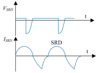
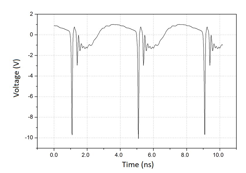
VI Characteristics of Step Recovery Diode (SRD):
The Voltage-Current (VI) characteristics of a Step Recovery Diode (SRD) are crucial for understanding its behavior under different operating conditions. These characteristics highlight how the diode responds to varying voltage and current levels, particularly emphasizing its unique ability to store and release charge rapidly.
Region of Forward Bias:
Forward Voltage (VF):
- In the forward bias region, the SRD behaves similarly to a standard diode. When a forward voltage is applied, current flows through the diode, and the voltage drop across the diode is relatively low, typically around 0.7 volts for silicon-based SRDs.
- As the forward current increases, the forward voltage drop increases slightly but remains within a limited range due to the exponential relationship between the forward current (IF) and the forward voltage (VF).
Forward Current (IF):
The forward current increases exponentially with the forward voltage. This relationship is described by the diode equation:
𝐼F = 𝐼S(eVF/nVT – 1)
where 𝐼S is the saturation current, n is the ideality factor, and VT is the thermal voltage.
Region of Reverse Bias:
Reverse Voltage (VR):
- When a reverse voltage is applied, the diode initially conducts until all stored charge carriers are swept out of the junction. This period is characterized by the reverse recovery time.
- After the stored charge is depleted, the diode enters the non-conducting state, and the current drops sharply. The reverse voltage can be increased up to the breakdown voltage of the diode without significant reverse current flow.
Reverse Current (IR):
- During the reverse recovery period, a transient reverse current flows as the stored charge carriers are removed. This reverse current is relatively high initially but drops rapidly as the charge is cleared.
- After the reverse recovery period, the reverse current stabilizes to a very low leakage current level, typical of a reverse-biased diode.
Key VI Characteristics:
- High-Speed Switching: The most distinctive feature of the SRD is its ability to switch from forward conduction to reverse non-conduction rapidly. This high-speed switching is evident in the sharp transition seen in the VI curve when moving from forward bias to reverse bias.
- Reverse Recovery Time (trr): The reverse recovery time is a critical parameter that defines the time it takes for the diode to stop conducting once the forward current is interrupted. This time is extremely short for SRDs, typically in the range of picoseconds to nanoseconds, enabling their use in high-frequency applications.
- Charge Storage and Release: The SRD’s ability to store and quickly release charge during the transition from forward to reverse bias is a key aspect of its VI characteristics. This behavior is crucial for generating sharp pulses and high-frequency harmonics.
VI Curve Illustration:
The VI characteristics curve of an SRD can be divided into three main regions: forward conduction, reverse recovery, and reverse non-conduction.
- Forward Conduction Region: Shows an exponential increase in current with increasing forward voltage.
- Reverse Recovery Region: Indicates a transient reverse current as the stored charge is cleared from the junction.
- Reverse Non-Conduction Region: Exhibits very low leakage current once the stored charge is depleted and the diode is fully reverse biased.
Advantages of Step Recovery Diode (SRD):
High-Speed Performance:
SRDs are capable of extremely fast switching, with transition times typically in the range of picoseconds to nanoseconds. This makes them ideal for high-frequency applications where rapid transitions are essential.
Sharp Pulse Generation:
The ability to generate very narrow and high-amplitude pulses is one of the key advantages of SRDs. This characteristic is crucial for applications like pulse shaping, radar systems, and communication technologies.
Efficient Harmonic Generation:
SRDs are highly efficient in generating harmonics, making them useful in frequency multiplication circuits. This capability is important for creating higher frequency signals from a lower frequency input.
Low Junction Capacitance:
SRDs exhibit low junction capacitance, which is beneficial for high-frequency operations. Lower capacitance helps in minimizing signal distortion and improving overall circuit performance.
Compact Size:
The compact size of SRDs makes them suitable for integration into modern electronic circuits where space is at a premium.
Disadvantages of Step Recovery Diode (SRD):
Complex Fabrication:
The manufacturing process of SRDs is more complex compared to conventional diodes. This complexity can lead to higher production costs and may require more sophisticated equipment and techniques.
Limited Power Handling:
SRDs are not designed for high-power applications. They have limited thermal dissipation capabilities, which restricts their use to low-power circuits. Overloading an SRD can lead to overheating and potential failure.
Sensitivity to Operating Conditions:
The performance of SRDs can be highly sensitive to operating conditions such as temperature and biasing. Proper design and implementation are required to ensure stable operation and to avoid performance degradation.
Higher Cost:
Due to their specialized fabrication process and material requirements, SRDs are generally more expensive than standard diodes. This higher cost can be a consideration in cost-sensitive applications.
Limited Availability:
SRDs are not as widely available as conventional diodes. Finding specific models or replacements can sometimes be challenging, especially for specialized applications.
Applications of Step Recovery Diode:
Step Recovery Diodes (SRDs) are versatile components in high-frequency electronics due to their rapid switching capabilities and ability to generate sharp pulses. Here are some of the primary applications of SRDs:
1. Frequency Multipliers
SRDs are commonly used in frequency multipliers, which are circuits designed to produce harmonics of an input signal. The sharp transition characteristics of SRDs help generate higher-frequency signals from a given input frequency.
- Radio Frequency (RF) and Microwave Frequency Multipliers: In RF and microwave communication systems, SRDs help generate higher frequencies from a fundamental frequency, facilitating efficient signal transmission over long distances.
2. Pulse Generators
Pulse generators require components that can switch states rapidly and generate narrow, high-amplitude pulses. SRDs are ideal for this purpose due to their fast recovery times.
- Radar Systems: In radar technology, precise timing and rapid pulse generation are crucial. SRDs help in generating the necessary pulses for radar signal processing.
- Digital Communications: In digital communication systems, SRDs assist in creating precise timing signals required for data transmission and synchronization.
3. Harmonic Generation
The ability of SRDs to generate sharp pulses makes them suitable for harmonic generation. Harmonics are integral multiples of a fundamental frequency and are used in various applications.
- Spectrum Analysis: Harmonic generation using SRDs aids in spectrum analysis, allowing for the study and characterization of signal properties across different frequency ranges.
- Signal Processing: In advanced signal processing, harmonics generated by SRDs are used to improve signal clarity and fidelity.
4. Microwave Mixers and Oscillators
SRDs are used in the design of microwave mixers and oscillators, essential components in RF and microwave systems.
- Mixers: In microwave mixers, SRDs help convert frequencies by mixing two signals to produce new frequencies, facilitating signal processing in communication systems.
- Oscillators: SRDs contribute to the stability and performance of microwave oscillators, which generate stable frequency signals for various applications, including communication and instrumentation.
5. Phase Shifters
In phased array antennas and other RF applications, precise control over the phase of a signal is required. SRDs are used in phase shifters to achieve this control due to their fast switching capabilities.
- Phased Array Antennas: SRDs help in adjusting the phase of individual antenna elements, enabling beam steering and improved signal reception.
6. Pulse Compression and Stretching
SRDs are used in pulse compression and stretching techniques, which are crucial in radar and communication systems for improving signal resolution and detection capabilities.
- Radar Signal Processing: Pulse compression using SRDs enhances radar resolution, allowing for more accurate target detection and tracking.
- Communication Systems: Pulse stretching techniques involving SRDs help manage signal timing and synchronization, improving data integrity and transmission efficiency.
7. Test and Measurement Equipment
In test and measurement equipment, SRDs are used to generate precise timing signals and sharp pulses, essential for accurate testing and characterization of electronic components and systems.
- Oscilloscopes: SRDs are employed in oscilloscopes to generate reference pulses for accurate time-base calibration.
- Signal Generators: In signal generators, SRDs help produce high-frequency test signals required for various testing scenarios.
Conclusion:
The Step Recovery Diode (SRD) is a crucial component in high-frequency and fast-switching applications due to its unique ability to store and release charge quickly. Its distinct Voltage-Current (VI) characteristics, such as rapid switching from forward conduction to reverse non-conduction, minimal reverse recovery time, and efficient charge storage, make it ideal for generating sharp pulses and high-frequency harmonics. Understanding these properties enables the effective use of SRDs in advanced electronic circuits and systems, highlighting their significance in modern electronics.