Bipolar Junction Transistors (BJT) are widely used for amplification and switching purposes. It consists of three layers of doped material, forming two PN junctions. These layers are called the emitter, base, and collector. There are two main types of BJTs: NPN and PNP, which differ in the arrangement and type of charge carriers involved.
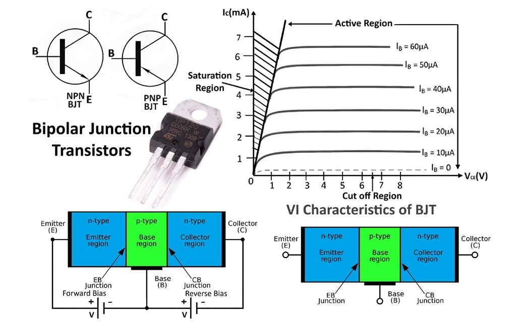
Symbol of BJT:
The symbol of a BJT varies based on its type (NPN or PNP). Here are the symbols:
- NPN Transistor: The arrow on the emitter points outwards.
- PNP Transistor: The arrow on the emitter points inwards.

Types of BJT:
There are two main types of BJTs:
- NPN Transistor
- PNP Transistor
Bipolar Junction Transistors (BJT) Construction:
A Bipolar Junction Transistor (BJT) is a type of transistor that uses both electron and hole charge carriers. BJTs are made up of three layers of semiconductor material, forming two p-n junctions. There are two types of BJTs: NPN and PNP. Here’s a detailed look at their construction:

NPN Transistor:
Emitter (E):
- Heavily doped with N-type material.
- Emits electrons into the base.
Base (B):
- Thin and lightly doped with P-type material.
- Controls the number of electrons passing through.
Collector (C):
- Moderately doped with N-type material.
- Collects electrons from the base.

PNP Transistor:
Emitter (E):
- Heavily doped with P-type material.
- Emits holes into the base.
Base (B):
- Thin and lightly doped with N-type material.
- Controls the number of holes passing through.
Collector (C):
- Moderately doped with P-type material.
- Collects holes from the base.
Physical Structure:
- Layers: In both NPN and PNP transistors, the layers are arranged in the sequence of emitter, base, and collector.
- Doping Levels: The emitter is heavily doped to inject a high number of charge carriers. The base is thin and lightly doped to allow most carriers to pass through to the collector. The collector is moderately doped and larger in size to collect the carriers.
Working Principle of BJT:
- NPN Transistor: When a small positive voltage is applied to the base-emitter junction, electrons are injected from the emitter into the base. Because the base is thin and lightly doped, most electrons pass through to the collector, creating a current flow from the collector to the emitter.
- PNP Transistor: When a small negative voltage is applied to the base-emitter junction, holes are injected from the emitter into the base. These holes pass through the base to the collector, creating a current flow from the emitter to the collector.

Biasing of BJT:
- Active Region: The emitter-base junction is forward-biased, and the collector-base junction is reverse-biased.
- Cut-off Region: Both the emitter-base and collector-base junctions are reverse-biased.
- Saturation Region: Both the emitter-base and collector-base junctions are forward-biased.
VI Characteristics of Bipolar Junction Transistors:
The Voltage-Current (VI) characteristics of Bipolar Junction Transistors (BJTs) are essential to understanding their operation. BJTs are three-layer semiconductor devices consisting of either an NPN or PNP configuration. The VI characteristics describe the relationship between the currents and voltages at the different terminals of the BJT (collector, base, and emitter).
VI Characteristics of NPN BJT:
Input Characteristics (Base-Emitter Junction):

- Configuration: Common Emitter (CE)
- Plot: Base current (I_B) vs. Base-Emitter voltage (V_BE)
- Behavior: Similar to a forward-biased diode. As V_BE increases, I_B increases exponentially.
Output Characteristics (Collector-Emitter Junction):
- Configuration: Common Emitter (CE)
- Plot: Collector current (I_C) vs. Collector-Emitter voltage (V_CE) for various base currents (I_B).
- Regions:
- Cutoff Region: Both junctions are reverse-biased. I_C is almost zero.
- Active Region: Base-Emitter junction is forward-biased, and Collector-Base junction is reverse-biased. I_C is primarily determined by I_B (I_C ≈ β * I_B).
- Saturation Region: Both junctions are forward-biased. I_C increases very little with V_CE increase.

- Behavior:
- For a given I_B, as V_CE increases, I_C initially increases and then saturates (remains constant) in the active region.
- In the saturation region, further increases in V_CE have a minimal effect on I_C.
VI Characteristics of PNP BJT:
Input Characteristics (Base-Emitter Junction):
- Configuration: Common Emitter (CE)
- Plot: Base current (I_B) vs. Base-Emitter voltage (V_BE)
- Behavior: Similar to a forward-biased diode but with reverse polarity compared to NPN. As V_BE (negative) increases in magnitude, I_B increases exponentially.

Output Characteristics (Collector-Emitter Junction):
- Configuration: Common Emitter (CE)
- Plot: Collector current (I_C) vs. Collector-Emitter voltage (V_CE) for various base currents (I_B).
- Regions:
- Cutoff Region: Both junctions are reverse-biased. I_C is almost zero.
- Active Region: Base-Emitter junction is forward-biased, and Collector-Base junction is reverse-biased. I_C is primarily determined by I_B (I_C ≈ β * I_B).
- Saturation Region: Both junctions are forward-biased. I_C increases very little with V_CE increase.
- Behavior:
- For a given I_B, as V_CE increases (negative direction), I_C initially increases and then saturates (remains constant) in the active region.
- In the saturation region, further increases in V_CE have a minimal effect on I_C.
Key Points to Remember:
- Common Emitter Configuration is widely used due to its amplification properties.
- I_C depends on I_B and the current gain β in the active region.
- V_BE typically has a threshold (around 0.7V for silicon BJTs) to turn on the BJT.
- The Saturation Region is used for switching applications (transistor acts as a closed switch).
- The Active Region is used for amplification applications.
Understanding these characteristics helps in designing and analyzing circuits involving BJTs for various electronic applications.
Advantages and Disadvantages of Bipolar Junction Transistors:
Here are some advantages and disadvantages of BJTs:
Advantages of BJT:
- High Gain: BJTs can provide high current and voltage gain, making them suitable for amplification purposes.
- Good Frequency Response: BJTs generally have a good frequency response, which is beneficial for high-frequency applications.
- Ease of Biasing: They are relatively easier to bias compared to other types of transistors, which simplifies circuit design.
- Low Saturation Voltage: BJTs have a low saturation voltage, which results in lower power dissipation when they are in the on state.
- Thermal Stability: BJTs can be more thermally stable compared to some other transistor types, which helps in maintaining performance over a range of temperatures.
- Analog Applications: They are highly suitable for analog applications, such as amplifiers, because of their linear response characteristics.
Disadvantages of BJT:
- Power Consumption: BJTs generally consume more power than Field-Effect Transistors (FETs) when operating in high-frequency circuits.
- Heat Generation: Due to higher power consumption, BJTs tend to generate more heat, which may require additional cooling mechanisms.
- Lower Input Impedance: BJTs have lower input impedance compared to FETs, which can load the preceding stage in a circuit and affect performance.
- Complex Biasing: While biasing is generally easier, for specific applications, BJTs might require more complex biasing networks to achieve the desired operating point.
- Switching Speed: BJTs are generally slower in switching compared to FETs, making them less suitable for high-speed digital applications.
- Device Size: BJTs are often larger than equivalent FETs, which can be a disadvantage in integrated circuits where space is a premium.
- Current Control: BJTs are current-controlled devices, meaning they require a continuous input current to remain on, which can be less efficient in some applications compared to voltage-controlled devices like FETs.
Applications of Bipolar Junction Transistors:
Bipolar Junction Transistors (BJTs) are widely used in various electronic applications due to their ability to amplify currents and switch signals. Here are some key applications of BJTs:
Amplifiers:
Audio Amplifiers: BJTs are used in audio amplification circuits to boost weak audio signals to a level suitable for driving speakers.
RF Amplifiers: In radio frequency (RF) applications, BJTs amplify weak RF signals in communication devices like radios and televisions.
Switching:
Digital Circuits: BJTs are used as switches in digital circuits to turn on and off electrical signals.
Power Switches: High-power BJTs can switch large currents and voltages, making them suitable for use in power supply circuits and motor controllers.
Oscillators:
BJTs are employed in oscillator circuits to generate periodic signals, such as in signal generators and clock circuits for digital systems.
Signal Modulation:
In communication systems, BJTs are used in modulation circuits to encode information onto carrier signals.
Voltage Regulation:
BJTs are used in voltage regulator circuits to maintain a constant output voltage despite variations in input voltage or load conditions.
Current Sources:
BJTs can be configured to provide a constant current to a load, which is useful in various analog circuits.
Temperature Sensing:
Due to their predictable change in voltage with temperature, BJTs can be used in temperature sensing and compensation circuits.
Analog and Mixed-Signal Circuits:
BJTs are used in a variety of analog and mixed-signal circuits, including operational amplifiers, analog-to-digital converters, and digital-to-analog converters.
Darlington Pair:
Two BJTs can be connected to form a Darlington pair, which provides high current gain and is used in applications requiring high amplification.
Current Mirrors:
BJTs are used in current mirror circuits to replicate a current from one branch of a circuit to another, ensuring consistent current flow.
LED Drivers:
BJTs can drive LEDs by providing the necessary current to illuminate them.
Motor Control:
BJTs are used in motor control circuits to regulate the power supplied to motors, controlling their speed and direction.
BJTs continue to be an essential component in many electronic devices and systems due to their versatility and performance characteristics.
BJT Summary:
- Types: NPN and PNP transistors.
- Construction: Consists of emitter, base, and collector with different doping levels.
- Working: Based on the control of current flow through the base-emitter and base-collector junctions.
- Applications: Amplifiers, switches, oscillators, regulators, and analog circuits.
Understanding these aspects of BJTs helps in their effective utilization in electronic circuit design.
JFET Junction Field Effect Transistors Working and Applications