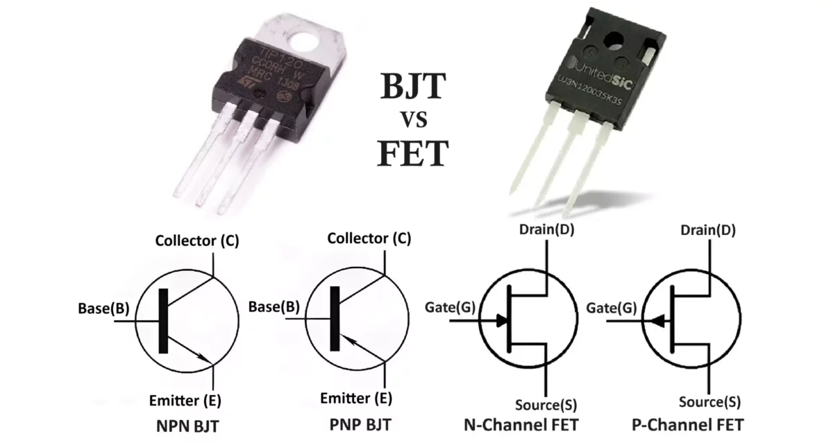
This article delves into the core differences between BJT and FET. In electronics, transistors are the building blocks of modern electronic devices. They act as switches, amplifiers, and signal modulators in a wide variety of applications.
Among transistors, Bipolar Junction Transistors (BJT) and Field Effect Transistors (FET) are two of the most widely used types. While they share similarities in their ability to control current, their operation, construction, and characteristics are significantly different. You can also see difference between BJT and MOSFET.
What is a BJT?
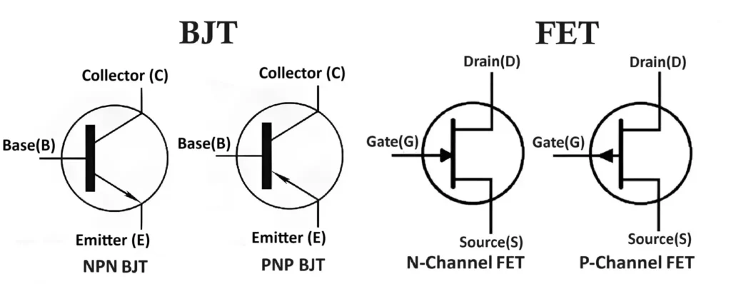
A Bipolar Junction Transistor (BJT) is a type of transistor that relies on the movement of both electrons and holes to conduct current. It has three terminals:
- Emitter (E): The emitter is the terminal responsible for injecting charge carriers (electrons or holes) into the base. It is heavily doped to provide a high concentration of carriers.
- Base (B): The base is a thin, lightly doped layer that serves as the control region for the transistor. A small current or voltage applied to the base controls the flow of carriers between the emitter and collector.
- Collector (C): The collector is the terminal that collects the charge carriers from the emitter through the base. It is moderately doped and larger in size compared to the emitter to handle a higher amount of current.
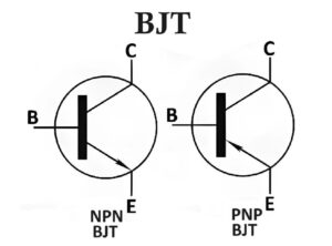
BJTs come in two types: NPN and PNP. In an NPN transistor, current flows from the collector to the emitter when a small current is applied to the base. In a PNP transistor, the direction of current flow is reversed.
The key principle of operation for a BJT is that a small current at the base terminal controls a larger current between the collector and emitter terminals. This property makes BJTs suitable for amplification applications.
Structure and Operation:
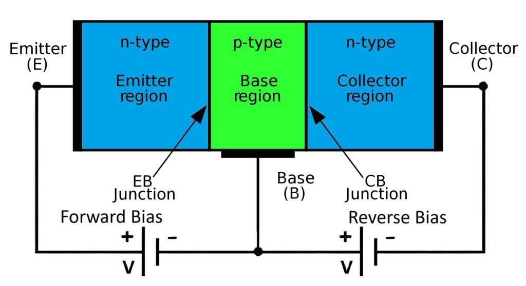
The BJT is constructed with three layers of semiconductor material that form two p-n junctions:
- NPN Transistor: The layers are arranged as n-type, p-type, and n-type. In this configuration, electrons are the majority carriers, and holes are the minority carriers.
- PNP Transistor: The layers are arranged as p-type, n-type, and p-type. Here, holes are the majority carriers, and electrons are the minority carriers.
When a small current flows into the base of an NPN transistor, it reduces the barrier for electron flow from the emitter to the collector. This amplification of current makes BJTs highly effective for various electronic applications.
Characteristics of BJTs:
- Current-Controlled Device: The output current is controlled by the input current at the base.
- High Gain: A small input current at the base can control a much larger current flowing from the collector to the emitter.
- Low Input Impedance: The base requires a continuous supply of current, resulting in lower impedance compared to FETs.
- Thermal Instability: BJTs are susceptible to thermal runaway due to their positive temperature coefficient.
Advantages of BJTs:
- High current gain, making them ideal for amplification.
- Simple design and construction.
- Good linearity for analog applications.
- Suitable for low-frequency and low-power applications.
- Widely available and cost-effective.
Disadvantages of BJTs:
- Higher power consumption due to the continuous base current.
- Lower input impedance compared to FETs.
- Prone to thermal instability at high power levels.
- Limited switching speed for high-frequency applications.
- Requires more biasing components in the circuit design.
What is an FET?
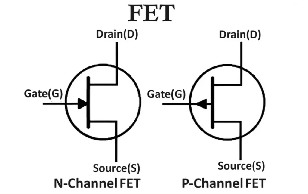
A Field Effect Transistor (FET) is a type of transistor that controls current through the use of an electric field. Unlike BJTs, FETs are unipolar devices, meaning they rely on either electrons (n-channel) or holes (p-channel) for conduction. FETs have three terminals:
- Source (S): The source is the terminal through which charge carriers (electrons or holes) enter the channel. It is analogous to the emitter in a BJT and is the starting point for current flow in the FET.
- Gate (G): The gate is the control terminal that regulates the flow of current between the source and drain. By applying a voltage to the gate, an electric field is created, which modulates the conductivity of the channel. This is analogous to the base in a BJT but does not require a continuous current.
- Drain (D): The drain is the terminal where charge carriers exit the channel. It is analogous to the collector in a BJT and serves as the output terminal for the FET.
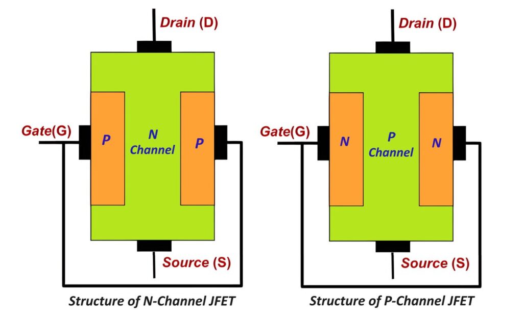
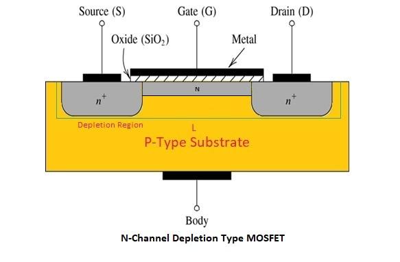
FETs come in several types, the most common being the Junction Field Effect Transistor (JFET) and the Metal-Oxide-Semiconductor Field Effect Transistor (MOSFET). In a FET, the voltage applied at the gate terminal controls the current flow between the source and drain terminals. The high input impedance of FETs makes them ideal for applications requiring minimal current draw from the signal source.
Structure and Operation:
FETs are constructed with a semiconductor channel through which current flows, controlled by an electric field generated at the gate terminal. There are two main types of FETs:
- Junction Field Effect Transistor (JFET): The gate is connected to the channel via a pn-junction. When a reverse voltage is applied to the gate, the channel narrows, reducing current flow.
- Metal-Oxide-Semiconductor Field Effect Transistor (MOSFET): The gate is insulated from the channel by a thin layer of oxide, making it a voltage-controlled device. MOSFETs come in two modes: enhancement mode and depletion mode.
In n-channel FETs, electrons are the majority carriers, and current flows from the source to the drain. In p-channel FETs, holes are the majority carriers, and the current direction is reversed.
Characteristics of FETs:
- Voltage-Controlled Device: The output current is controlled by the voltage applied at the gate terminal.
- High Input Impedance: The gate draws negligible current, making FETs suitable for high-impedance applications.
- Low Power Consumption: Due to the lack of significant gate current, FETs consume less power compared to BJTs.
- Thermal Stability: FETs are more thermally stable, with a negative temperature coefficient that reduces current at higher temperatures.
Advantages of FETs:
- High input impedance reduces loading on preceding stages.
- Low power consumption due to negligible gate current.
- Better thermal stability.
- Suitable for high-frequency applications due to faster switching.
- Compact size allows integration into large-scale ICs.
- Greater efficiency in digital circuits.
Disadvantages of FETs:
- Lower gain compared to BJT.
- Susceptible to damage from static electricity, especially MOSFETs.
- More expensive and complex to manufacture.
- Limited output current handling in some applications.
- Requires precise gate voltage control to avoid damage.
Key Differences Between BJT and FET
| Aspect | BJT | FET |
|---|---|---|
| Current Control vs Voltage Control | BJTs are current-controlled devices. A small base current controls a larger collector-emitter current. | FETs are voltage-controlled devices. A gate-source voltage controls the drain-source current. |
| Carrier Type | Bipolar device (uses both electrons and holes). | Unipolar device (uses either electrons or holes). |
| Input Impedance | Low input impedance due to base current. | High input impedance, typically in the megaohms range. |
| Power Consumption | Higher power consumption because of continuous base current. | Lower power consumption as gate draws negligible current. |
| Switching Speed | Moderate switching speed. | Faster switching speed, especially for MOSFETs. |
| Thermal Stability | Less thermally stable; prone to thermal runaway. | More thermally stable due to negative temperature coefficient. |
| Gain | High current gain (hFE). | Lower current gain but high voltage gain. |
| Construction Complexity | Simpler structure, easier to manufacture. | More complex structure, especially for MOSFETs. |
| Noise | Generates more noise due to low input impedance. | Less noise, making it suitable for high-frequency applications. |
| Operating Principle | Relies on both electrons and holes for conduction. | Relies on either electrons or holes for conduction. |
| Physical Size | Typically larger in size for high-power applications. | More compact, especially MOSFETs used in ICs. |
| Response Time | Slower in response to input signal changes. | Faster response time due to low capacitance at the gate. |
| Damage Susceptibility | More robust against static discharge. | Prone to damage from static electricity, especially MOSFETs. |
| Application Area | Ideal for analog applications like amplification. | Dominant in digital circuits and high-frequency applications. |
| Biasing | Requires proper biasing of the base-emitter junction. | Simple gate voltage biasing; no current flow into the gate. |
| Cost | Generally less expensive and simpler to manufacture. | Slightly more expensive due to complex fabrication processes. |
| Example | BC547, 2N3904 | 2N5457, IRFZ44N |
Applications of BJT and FET
BJT Applications:
- Analog amplifiers
- Oscillators
- Low-frequency circuits
- Audio amplification
- Switching applications in low-power circuits
FET Applications:
- Digital circuits (e.g., CMOS technology)
- High-frequency amplifiers
- Power electronics (e.g., SMPS, motor controllers)
- RF circuits
- Battery-operated devices due to low power consumption
Conclusion
While both BJTs and FETs are indispensable components in electronics, their fundamental differences make them suitable for different applications. BJTs excel in analog and low-frequency applications due to their high gain, while FETs dominate in digital, high-frequency, and power-efficient circuits due to their high input impedance and fast switching capabilities. Understanding the characteristics and limitations of each type is crucial for selecting the right transistor for a specific application.
Types of Transistors: Classification (BJT, JFET, MOSFET & IGBT)
