Components Required for FM Transmitter:
R1 2.7k (1/4watt)
R2, R3 27K (1/4watt)
R4 1k (1/4watt)
R5 4.7k (1/4watt)
R6 100R (1/2watt)
C1 0.047uF
C2 10uF
C3 0.5uF
C4 0.2uF
C5 5pF
C6 variable capacitor 45pF
C7 0.022uF
Q1, Q2 BC547 (NPN Transistor)
M1 microphone
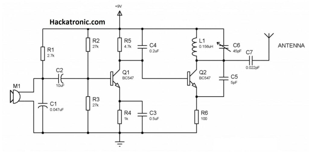
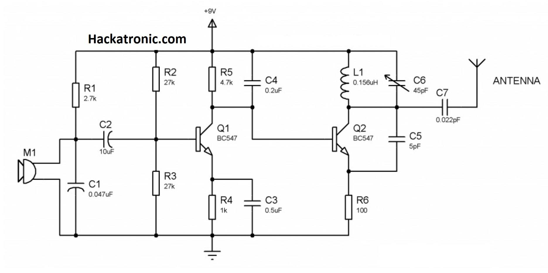
FM Transmitter Circuit Diagram:

Working and Connection of Circuit:
The circuit consists of few discrete components. The audio signal is picked up by the microphone which converts the signal into a voltage waveform. This signal is then fed to the transistor Q1 after blocking the DC component. Capacitor C2 blocks the DC component while allowing the AC component to pass. Transistor Q1 amplifies this signal. This stage is a common-emitter stage. This stage is used here to amplify the signal.
Transistor Q2 is wired as an oscillator operating in the FM band. This stage generates the carrier’s frequency on which the audio signal has to travel. This oscillator stage consists of an inductor and a variable capacitor. They oscillate at their resonant frequency which is in the FM band. Capacitor C7 couples the FM signal to the Antenna and blocks the DC part to avoid any distortion. The circuit is powered from any 9V DC source. To get the battery performance, a 9V DC battery is preferred or a very low noise DC source.
The antenna can be a 1-meter long wire. The inductor L1 can be made by making 6 turns of 0.8mm enameled copper wire on a 5.5mm diameter/4.5mm length plastic former. By proper tuning the circuit and with a matching antenna, this transmitter can have a range of up to 100 meters. To make this circuit perfect, you need to make it on PCB. The copper trace should be small enough to avoid stray inductance. SMD components are preferred to the DIP.

This article is nice for. I there for wish to join you
What is the range of the circuit. it will work?
Can’t say
I will work
Iam doing a project of this. The circuit will work?
Please help me to do this project. Iam taking your circuit
Ok share your experience after making this circuit