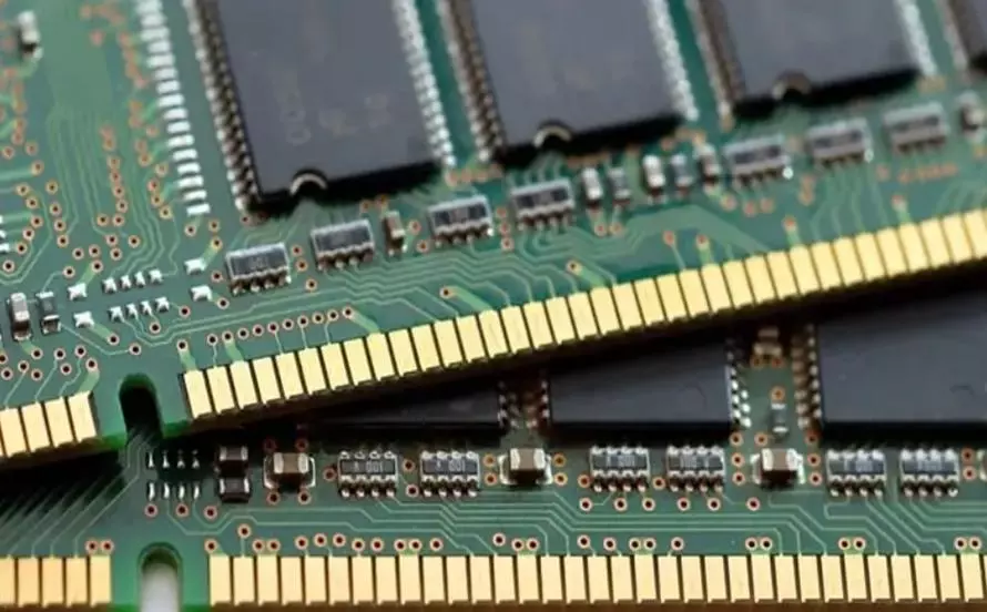
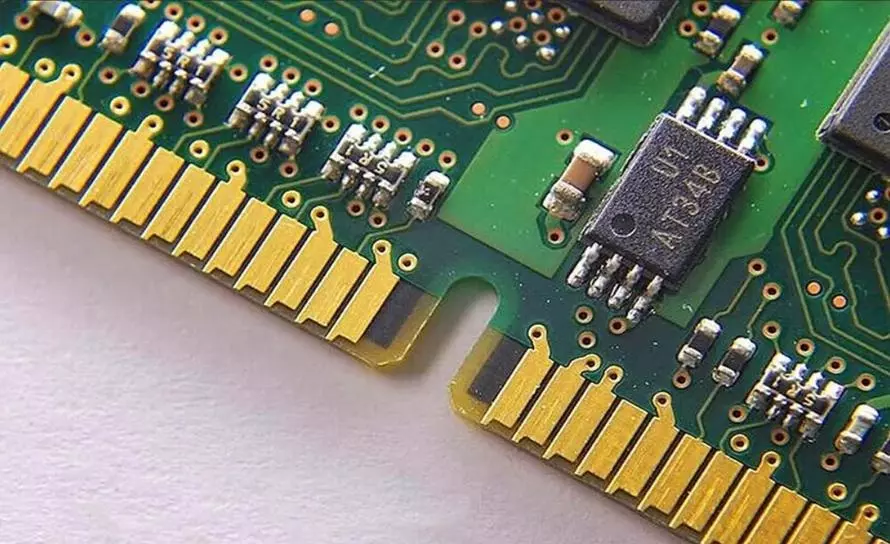
Gold Finger PCB assembly requires the construction of edge connectors with gold finishing, making it possible to get the best electrical connections over other connections between circuit boards. This process is primary in electronic equipment because connection integrity is important in every device.
Gold plating of high quality provides good conductivity and greater wear and corrosion resistance, which is highly recommended for applications involving frequent insertion and removal.
This article will discuss gold finger PCB assembly. It will also highlight the best practices to ensure reliability during the process.
Gold Fingers in PCB Assembly
Gold fingers are the gold-plated area on the edge of the printed circuit board (PCB) that allows for connection to another board or component. Its function is to create a stable, highly conductive relationship crucial in making end-to-end and long-term connections to various devices.
The gold plating makes these connectors anti-corrosive and relatively resistant to wearing out, a highly desirable characteristic, especially for applications in which connection and disconnection frequently occur.
Gold fingers are widely used in computer motherboards, expansion cards, and other types of connections in the telecommunication industry. They are also frequently applied to equipment where safe, stable connections are important, particularly in medical and aerospace equipment. Gold Fingers has the critical function of preserving the usability of electronic systems by enhancing communication integrity.

Best Practices to Ensure Reliability
Importance of Reliable Gold Finger PCB Assembly
Look for a reputable Gold Finger PCB assembly service to get the work done correctly. High-quality Gold Fingers also possess conductivity, wear, and corrosion resistance, which are crucial for stabling and lasting connectivity. This is most important in devices that are inserted and removed frequently because connection reliability greatly affects functionality.
Some of the industries that could not afford to have any failure in Gold Finger PCB assembly include those that deal with computers and their peripherals. The motherboard, where Gold Fingers are used to connect expansion cards, is a sensitive product that cannot afford to fail, hence its manufacturing process must meet high standards to guarantee success. Regarding medical devices, good connections are mandatory to diagnose and provide proper protection for the patient.
Aviation technology also uses commensurate Gold Finger connections for various systems installed onboard aircraft. Maintaining the dependable PCB assembly of Gold Finger also enables avoiding failures that lead to enhancing the device’s performance and the lifespan of the vital circuits in electronic devices.
Choosing the Right Materials
The proper choice of materials is important for the reliability of Gold Finger PCB assemblies. The materials used directly influence the connections’ durability, conductivity, and performance. The materials used in making the Gold Fingers must be of high quality to ensure they do not degrade when inserted and removed frequently.
The recommendations for base materials for Gold Finger PCBs include high-quality materials such as the well-acclaimed FR4. Generally, for the gold plating, a nickel underlayer is applied to improve the adhesion, and then the pure gold layer with a purity of 99. 7% or higher is applied. This high-purity gold has better electrical conductivity and good anti-corrosion and wear-resistant performance.
It’s possible to note that the benefits resulting from using high-quality gold plating are numerous. It also guarantees optimal contact, especially concerning the electrical conductivity that is fundamental for the stability of connections.
Moreover, gold does not degrade over time. It is less likely to corrode, making the electronic connection last longer without developing issues with the environment in which it is placed.
Design Considerations for Gold Finger PCBs
Some design elements must be carefully considered to design a durable and efficient Gold Finger PCB. Some of them are the thickness and the quality of the gold plating performed on the metallic substrate.
The gold plating thickness should be not less than 30 micro-inch as its endurance and conductivity determine the quality of the critical design element. It is also necessary to consider the bevel angle of the Gold Fingers. Usually, they must be placed at 30 to 45 degrees for easy insertion and removal.
To achieve the correct layout and dimension, the Gold Fingers must be well-spaced and well-aligned to avoid misalignment when inserting them. Generally, a pitch carried to a uniform standard of about one is used in this type of motor. Standard acrylic is 1.27mm (50 mils), depending on the application. It also becomes easy to create correct spacing that reduces the possibility of signal interferences or cross-talk between the connections.
Learn from design pitfalls, which can include inadequate thickness of gold, wrong beveling, and wrong spacing, which lead to low contact reliability and wear. Furthermore, physical characteristics, such as chamfered edges, need to be incorporated into the PCB layout to avoid subjecting the device to mechanical damage while in use.
Manufacturing Best Practices
Making the gold finger PCBs requires some key and complex steps to produce the best assembly circuits. This is involved in the manufacturing process, where the PCB layout is created first, and then the actual printed circuit board is made of suitable materials such as FR4.
Next, a layer of nickel is deposited to the edge connectors to improve adherence. Then gold is plated, often by electroplating techniques, with a plating thickness of at least 30 micro inches of gold.
If they are allowed throughout the manufacturing process, the lack of quality control measures is unforgivable.
These are to inspect the PCB board’s gold plating for evenness and thickness, the efficiency of Gold Fingers conductivity, and ensure proper positioning and measurements to avoid connection problems. AOI and electrical tests can be used to inspect for defects.
It is about being accurate during manufacturing. This includes strict and rigorous process standards, good-quality plating solutions, and high-tech technical personnel to manage delicate plating and assembling.
An accurate manufacturing process helps provide the Gold Finger PCBs with high reliability and high performance for the applications.
Testing and Quality Assurance
Testing in all these aspects is critical in determining the overall quality and performance of the Gold Finger PCBs. This testing confirms that the PCBs are made to a certain quality and can be used multiple times without breaking down. Several key tests have to be carried out to ensure the Gold Fingers’ functionality.
This includes the tests of electrical conductivity to ensure that the gold fingers offer stable and efficient connections, and the other test is the wear/bearing resistance for gold plating.
Quality assurance is carried out in different stages of production, which includes inspection and tests of the manufacturing procedures. Quality assurance includes checks like AOI and functional tests. In AOI, visual inspection is carried out using cameras to detect any defects in the PCB. Functional testing is done to ensure the overall electrical functionality of the PCB.
Recording of tests periodically ensures that problems are detected on time, thus maintaining good quality. Some key considerations include designing high-quality Gold Finger PCBs that will not fail in critical applications due to poor quality.
Preventive Measures for Long-Term Reliability
Maintaining the integrity of Gold Fingers is crucial for long-term reliability. Cleaning regularly with isopropyl alcohol may help remove contaminants that may hamper conductivity. Do not use rough material that could scrape off the gold plating from the item’s surface.
Some maintenance practices include periodic checkups to determine the extent of deterioration or corrosion and whether the connectors have adequate contact for protection against physical damage. At the same time, applying a coat of varnish to Gold Fingers will protect them from moisture and oxidation.
Measures against the environmental category concern using anti-static bags to store PCBs and prevent and control humidity and temperature in storage and operating conditions. Adopting these measures goes a long way in improving the Gold Finger PCB’s lifespan and durability in the operational application.
Why Choose Viasion as your Gold Finger PCB Assembler?
Gold Finger PCB assemblies produced at Viasion are of the highest quality, enhancing reliability and performance. High-quality manufacturing services and quality control procedures ensure that all products are produced to the highest quality in the market. Some of the parts made are of standard materials. The Gold plating is of high purity for better conductivity and minimized wear and tear.
As a high-reliability interconnect solutions provider of Gold Finger PCBs for medical, Aerospace, telecommunication, etc., we ensure the proper functioning of the electrical circuits with repeated usage. Hence, our operational promise means creating only the best quality PCBs with high performance and durability. Engage Viasion for your PCB requirements and get futuristic products that offer smart solutions to ensure smooth device operation.
Conclusion:
In assuring the reliability of the Gold Finger PCB assembly, the best materials have to be used, the design has to be quite accurate, the manufacturing has to follow exact standards, and the components have to be tested thoroughly. These best practices are very important if the electronics and the other associated equipment are to work as expected and for as long as possible.
Revolutionary Axial Flux Printed Circuit Board (PCB) Stator Motor


