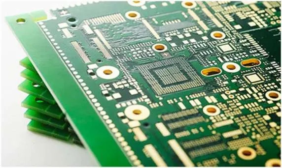
High Density Interconnect PCB (HDI) technology has quickly become a game-changer in the Printed Circuit Board (PCB) industry. With the increasing need for compact, high-performance electronics, the demand for HDI PCB has surged. HDI technology allows a higher density of components and interconnections to be placed on a PCB, leading to improved performance and functionality. This article explores how HDI technology is reshaping the PCB design and fabrication landscape.
What is HDI Technology?
At its core, HDI technology is about miniaturization. The relentless pace of technological advancements has necessitated smaller, more efficient PCBs. HDI boards contain finer lines and spaces, smaller capture pads, smaller vias, and higher connection pad densities than traditional PCBs.
Microvias, a hallmark of HDI boards, allow for more technology to be packed onto a smaller board. The result is a highly efficient PCB that meets the stringent requirements of modern electronics.
Driving Forces Behind the Adoption of HDI Technology
The adoption of HDI technology is not merely a passing trend, but rather a response to the evolving needs of the technology industry. Three key drivers fuel this transition.
Miniaturization:
With devices continually shrinking in size, there’s an increasing demand for more compact PCBs. HDI technology enables this miniaturization without compromising performance or reliability.
Increased Performance:
HDI boards offer superior performance, primarily due to shorter signal paths, which reduces signal loss and crosstalk.
Innovation in Electronics Design:
From smartphones to medical devices, the demand for more innovative and complex products is relentless. HDI technology enables the design complexity needed to drive these advancements.
Impact of High-Density Interconnect PCB Design
The implementation of HDI technology demands new design principles. Designers need to think in three dimensions, utilizing blind, buried, and microvias to interconnect layers and maximize space. HDI design requires careful consideration of trace and space widths, via size and placement, and layer stacking, as well as thermal management and signal integrity.
HDI Fabrication: Overcoming Challenges
Fabricating HDI PCBs is a more intricate process than traditional PCBs, requiring advanced manufacturing techniques and machinery. Laser drilling is commonly used for creating microvias, and sequential lamination allows for several rounds of lamination and drilling.
These techniques demand high precision and quality control. Despite these challenges, the benefits of HDI boards—smaller size, improved performance, and the capacity for design complexity—far outweigh the difficulties in fabrication.
The Future of HDI Technology
The influence of HDI technology on PCB design and fabrication is evident, and it will continue to drive the industry’s evolution. Future developments in HDI technology may allow even greater component and interconnect densities, pushing the boundaries of PCB miniaturization further. Additionally, improvements in HDI fabrication techniques will enhance efficiency, reduce costs, and lead to wider adoption across various sectors.
Conclusion
In a world increasingly reliant on small, high-performing electronic devices, HDI technology plays a critical role. By revolutionizing PCB design and fabrication, HDI is creating new possibilities and setting the stage for future innovations in electronics technology. The journey of HDI has only begun, and the technology’s full potential is yet to be realized.

